|
The
CDSP-k2
Processor
Register model, hardware accelerator, and
instruction set
|
|
 |
Register Model:
The CDSP-k2 is a derivative of the CDSP family's basic architecture.
Following is an architectural description applicable to the CDSP-k2
customization option.
The r0, r1, r2 and r3 registers are 2x32 bits wide, accommodating
32-bit fixed point complex numbers. Each of the two fixed point real
numbers composing the complex number is represented in two's complement
format with 1 bit allocated for the sign and 31 bits for the fractional
part (see the number format Appendix for more details). In most cases,
arithmetic operations inside the CDSP are performed in complex numbers
format; however there are some no-nonsense exceptions when the contents
of these registers is interpreted as an integer number by discarding
the imaginary part and considering the real part as a 32-bit integer
instead of a fixed point number (one such case is when using a register
as a loop counter).
The r4, r5, r6, and r7 registers are data ports for the integrated
Butterfly/MAC unit; they are all 32-bit fixed point complex registers.
The "psr" register is the processor status register; it is 32 bits wide
(see following sections).
The "dsr" register is a special 32-bit dynamic shift amount register
(see following sections).
Index register x0 is the DataROM pointer; it is 13 bits wide (for 8KW
DataROM).
Index registers x1, x2, and x3 are the RAM pointers; they are 13 bits
wide (for 8KW offset addresses).
Index base registers b0, b1, b2, and b3, limit registers L0, L1, L2,
and L3, and increment registers n0, n1, n2, and n3 are used by the
various indexed addressing modes; they have the same width as their
corresponding DataROM/RAM index registers (see following sections).
The bar (base address register) is used in the biased addressing modes
(see following sections). It is 16 bits wide (for a 64KW RAM).
The pcr (program counter register) is the instruction pointer. It is 14
bits wide (for 16KW CodeROM).
The rsr (return from subroutine register) holds the return address of
the last subroutine call; it is the programmer's responsibility to save
it (stack it) if nested calls are needed. It has the width of the pcr.
Ports p and q are the processor communication ports; each port is
implemented as a pair of unidirectional data paths, one for data input
and one for data output, i.e. the processor actually hosts a p-in, a
p-out, a q-in, and a q-out port. Each of these ports is 32 bits wide.
Port k is the control and synchronization port (it's also implemented
as a pair of unidirectional data paths). It logically groups together a
number of processor status and control bits.
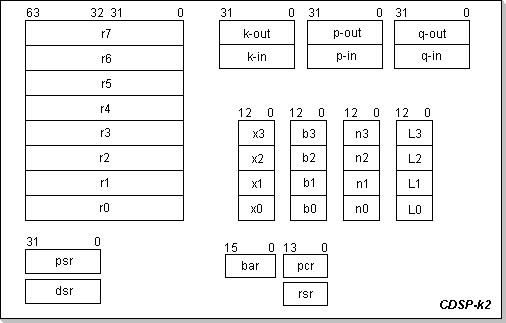
Figure 1: CDSP-k2 Registers (Programming Model)
Addressing Modes:
The instruction set is based on the two-operand model, one of them residing in a processor register, and the other residing in memory: RAM or DataROM (the CodeROM cannot be accessed as data). Most of the two-operand instructions follow this model, while most of the one-operand instructions operate on the internal registers only. These rules generate a highly orthogonal instruction set; however, some special-purpose instructions make exception from these rules (see following sections).
Following is a detailed description of the various addressing modes, accompanied by a number of relevant assembler examples.
Implied addressing:
This mode is used by instructions that either have no operand, or the
operand is implicitly specified by the instruction itself. Although the
basic processor instruction set only uses this mode for the "nop" and
"brk" control instruction, it is a useful option when implementing
application-specific instructions.
Assembler syntax example:
nop;        no operation (dummy instruction)
Direct addressing:
This mode specifies the data to be accessed by an instruction via its
address embedded in the instruction code. Both RAM and DataROM can be
accessed via this addressing mode. Depending on the operand type, the
assembler generates the correct instruction code format (RAM/DataROM
reference).
Assembler syntax example:
.cst k0: 123;   declare a constant, allocate a DataROM address for it, and define it as being 123
.var v0;        declare a variable and allocate a RAM address for it.
lda r0,k0;  r0 will be loaded with 123 (the k0 constant's address is supplied in the op-code)
lda r1,v0;  r1 will be loaded with v0 (the contents of the RAM location where v0 is allocated)
Remark:
The processor doesn't support in hardware the usual "immediate"
addressing mode; the assembler is responsible for converting the usual
assembler syntax specifying the immediate addressing mode into the
processor's DataROM direct addressing mode (a DataROM access is
inferred from the "immediate" mode):
lda r0,0.12:0.34    ;r0 will be loaded with the complex number 0.12+i*0.34
                    ;The assembler actually allocates an address in the DataROM,
                    ;places the 0.12+i*0.34 complex constant in that location,
                    ;and includes its address in the op-code.
Indexed addressing:
This mode specifies the data to be accessed by an instruction via its
address held in an index register. Both RAM and DataROM can be accessed
via this addressing mode. Depending on which index register is used to
point to the data, either the RAM or the DataROM is targeted.
Assembler syntax example:
lda r0,@x0; the DataROM location pointed by x0 is loaded into r0:  r0 = DataROM[x0]
lda r1,@x1; the RAM location pointed by x1 is loaded into r1:  r1 = RAM[x1]
Remark:
The index addressing mode is complemented with a number of related
features designed to enhance data access on typical DSP applications
(see following sections).
Indexed addressing variations:
The four index registers are featured with the following addressing
modes options:
Index register x0 DataROM pointer is featured with
post-increment and post-decrement options. Register n0 is used as a
signed variable increment/decrement. Wrap-around functionality is
provided. The following wrapping algorithm is used: first the data is
accessed via the post-increment or post-decrement mode; then the x0
index register is compared with the L0 limit register: if the values
match the index register is initialized with the b0 base register, else
it is incremented/decremented with the signed number in the increment
register n0.
Index registers x1, x2 and x3 RAM pointers are featured with the
post-increment, post-decrement, and bit-reversed addressing modes.
Wrap-around functionality is provided for the post-increment and
post-decrement modes by means of the related base (b2, b3) and limit
(L2, L3) registers; the wrapping algorithm is the same as described for
the x0 index register.
The bit-reversed mode updates the index registers (x) using the
corresponding increment (n) and limit registers (L) according to the
following algorithm: first (n)'s bit-reversed representation is added
to (x)'s bit-reversed representation, and the carry of this addition is
memorized (CY); then the result of this addition is bit-reversed back
to the proper order and loaded into (x); finally, if there was a carry
(CY) then the corresponding limit register (L) is added to the index
register (x) in order to provide the final result.
Assembler syntax example:
lda r0,@x0+     ;r0 = DataROM[x0], x0 = (x0 == L0 ? b0 : x0+=n0);
lda r1,@x1-     ;r1 = RAM[x1], x1 = (x1 == L1 ? b1 : x1-=n1);
lda r2,@x2*     ;r2 = RAM[x2], x2 = BitRev(BRSum=BitRev(x2)+BitRev(n2)), x2+=CY(BRSum)?L2:0;
Remark 1:
The relation between the index registers' limit (L) and base (b)
corresponding registers depends on the sign of the increment: it is up
to the programmer to ensure that for a positive increment L>b, while
for a negative increment L<b (here the increment stands for the
resulting amount by which the index register is updated, i.e. for a
negative "n" register and a post-decrement option, the resulting
increment is a positive number).
Remark 2:
The index registers have an associated "scan address space" when used
with the post-increment or post-decrement addressing modes, as defined
by their associated base (b) and limit (L) registers. Because the x
index registers are only checked for equality against their
corresponding limit register L in order to provide them with
wrap-around functionality, they will not wrap back to their base
address b if they pass over their limit address L without hitting it.
In order to guarantee that the wrap-around will consistently take
place, it is necessary to have (L-b) a multiple of the x index
registers' increment n, and x must be initialized with b. For example,
a valid configuration will be x3InitialValue=b3=10, n3=3, L3=22; this
will result in the following address space: {10, 13, 16, 19, 22}.
Biased addressing:
The bar register is a special purpose pointer that can be used to bias
both direct and indexed addressing modes, but only in conjunction with
RAM accessing (DataROM accesses cannot be biased). All the previously
discussed RAM addressing modes (and variations) have both the biased
and non-biased options.
Biased direct addressing mode:
When the bar register is used in conjunction with direct addressing,
the address supplied in the op-code is used as an offset (relative to
the bar) for accessing the data. This allows for a small address-field
in the operation code, while still enabling access to a large address
space by using a wide bar register. The address offset is interpreted a
signed number that is added to the bar register in order to provide the
final data address.
Assembler syntax example:
.var @10 v10    ;declare a variable by specifying it's address to be 10 (RAM location).
lda r1,bar:v10  ;r1 = RAM[bar+10]  // (v0 is interpreted as an offset; it can be seen as a local variable).
Biased indexed addressing mode:
When the bar register is used in conjunction with the index addressing
modes, the address held in the index registers is used as an offset
(relative to the bar) when accessing the data. The index register is
interpreted as a signed number that is added to the bar register in
order to provide the final data address.
Assembler syntax example:
ldx.ptr x1,10   ;load index register x1 with 10.
ldx.ptr x2,20   ;load index register x2 with 20.
lda r1,@bar:x1  ;load memory location RAM[bar+10] into r1.
lda r2,@bar:x2+ ;load memory location RAM[bar+20] into r2, then update x2.
Indirect addressing:
This is not a true addressing mode, but rather an addressing mode
modifier: a small group of instructions interpret their operand as the
address of the data they need to access. This modifier applies only to
the RAM addressing modes (direct and index variations, both biased and
unbiased). It is a convenient way of reducing the number of bits that
are required to provide a branch target address (by specifying a RAM
location that contains the branch address instead of specifying the
CodeROM address itself). This scheme also allows for calculated-address
branches, and makes possible the creation of return-address stacks in
RAM.
Assembler syntax example:
.var VariableBranchAddr    ; a number representing a CodeROM addr has to be placed in this var.
bri @VariableBranchAddr    ; the branch's CodeROM target address is now taken from this variable.
Instruction Set:
Table 1 lists the CDSP-k2 instruction set, together with the addressing modes applicable to each instruction.
Notations used in the instruction set table:
r - complex general purpose registers (r0 - r3) and the register-mapped
Butterfly/MAC unit (r4 - r7)
x - index registers (x0 - x3)
p - communication ports (the assembler names for the p and q DSP ports
are p0 and respectively p1)
t - memory operand, using any of the available addressing modes
(immediate, direct, indexed variations)
j - jump (and subroutine call) CodeROM address
N - immediate addressing mode (this is a pseudo addressing mode; the
assembler converts it to direct mode)
R - register operand
D - direct addressing mode
X -index addressing mode (and the index variations)
J - jump (and subroutine calls) CodeROM addressing mode
| Instruction Name | Mnemonic | Description | Addr. Modes | Remarks |
| No Operation | nop | pcr++ | - X | - |
| Logic AND | and r,t | Re[r] &= Re[t], Im[r] &= Im[t]; pcr++ | N D X | 1 |
| Logic Inclusive OR | ior r,t | Re[r] |= Re[t], Im[r] |= Im[t]; pcr++ | N D X | 1 |
| Logic Exclusive OR | xor r,t | Re[r] ^= Re[t], Im[r] ^= Im[t]; pcr++ | N D X | 1 |
| Addition | add r,t | r += t; pcr++ | N D X | 2 |
| Subtraction | sub r,t | r -= t; pcr++ | N D X | 2 |
| Reverse Subtraction | sbx r,t | r = t-r; pcr++ | N D X | 3 |
| Load dsr Dynamic Shift Register | lds.dsr t | dsr = Re[t], pcr++ | N D X | 4 |
| Dynamic Shift Left Arithmetic Reg | sla.dyn r,r | Re[r] <<<= dsr, Im[r] <<<= dsr; pcr++ | R | 4,5 |
| Dynamic Shift Left Arithmetic Location | sla.dyn r,t | Re[r] = Re[t] <<< dsr, Im[r] = Im[t] <<< dsr; pcr++ | D X | 4,5 |
| Shift Left Logic Register | sll.n r,r | Re[r] <<= n, Im[r] <<= n; pcr++ // n=1,2 | R | 2,5 |
| Shift Left Logic Location | sll.n r,t | Re[r] = Re[t] << n, Im[r] = Im[t] << n; pcr++ | D X | 2,5 |
| Shift Right Logic Register | srl.n r,r | Re[r] >>= n, Im[r] >>= n; pcr++ | R | 5 |
| Shift Right Logic Location | srl.n r,t | Re[r] = Re[t] >> n, Im[r] = Im[t] >> n; pcr++ | D X | 5 |
| Shift Right Arithmetic Register | sra.n r,r | Re[r] >>>= n, Im[r] >>>= n; pcr++ | R | 5 |
| Shift Right Arithmetic Location | sra.n r,t | Re[r] = Re[t]>>>n, Im[r] = Im[t]>>>n; pcr++ | D X | 5 |
| Swap Im with Re Register | sir r,r | Re[r] <-> Im[r]; pcr++ | R | - |
| Swap Im with Re Location | sir r,t | Re[r] = Im[t], Im[r] = Re[t]; pcr++ | D X | - |
| Load Accumulator | lda r,t | r = t; pcr++ | N D X | - |
| Store Accumulator | sta r t | t = r; pcr++ | D X | - |
| Load Processor Status Register | lds.psr t | psr = t; pcr++ | N D X | 6 |
| Store Processor Status Register | sts.psr t | t = psr; pcr++ | N D X | 6 |
| Test if Equal | teq r,t | Cmpf &= (r == t); pcr++ // Internal flag | N D X | 7 |
| Test if Not Equal | tne r,t | Cmpf &= (r != t); pcr++ | N D X | 7 |
| Test if Greater | tgr r,t | Cmpf &= (Re[r] > Re[t]); pcr++ | N D X | 7 |
| Test if Greater or Equal | tge r,t | Cmpf &= (Re[r]>= Re[t]); pcr++ | N D X | 7 |
| Test if Smaller | tsm r,t | Cmpf &= (Re[r] < Re[t]); pcr++ | N D X | 7 |
| Test if Smaller or Equal | tse r,t | Cmpf &= (Re[r] <= Re[t]); pcr++ | N D X | 7 |
| Test by Bitwise AND | tbw r,t | Cmpf &= Bool(r & t); pcr++ | N D X | 7,8 |
| Branch if True | brt j | Cmpf ? pcr = j : pcr++ | J | 9 |
| Branch if False | brf j | Cmpf ? pcr++ : pcr = j | J | 9 |
| Branch Always | bra j | pcr = j | J | - |
| Branch Indirect | bri @t | pcr = RAM[t] | D X | 10 |
| Cycle | cyc r,@t | Re[r]- -, Im[r]- -, Re[r] ? pcr = RAM[t] : pcr++ | D X | 11 |
| Hardware Repeat | rpt r,@t | D x | 12 | |
| Jump to Subroutine | jsr j | rsr = ++pcr; pcr = j | J | 13 |
| Store rsr register | sts.rsr t | t = rsr; pcr++ | D X | - |
| Load bar register | lds.bar t | bar = t; pcr++ | N D X | - |
| Store bar register | sts.bar t | t = bar; pcr++ | D X | - |
| Add to bar register | add.bar t | bar += t; pcr++ | N D X | 14 |
| Load comm output port | lds.com p,t | p-out = t; pcr++ | N D X | 15 |
| Store comm input port | sts.com p,t | t = p-in; pcr++ | D X | 15 |
| Load control output port | ctl t | k-out = t; pcr++ | N D X | 15 |
| Hardware Directed Break | brk | - | 16 | |
| Wait for Condition | wai t | N D X | 17 | |
| Register transfer to index pointer | xfr.ptr x,r | x.ptr = Re[r]; pcr++ | R | 18 |
| Load index pointer | ldx.ptr x,t | x.ptr = Re[t]; pcr++ | N D X | 19 |
| Store index pointer | stx.ptr x t | Re[t] = x.ptr; pcr++ | D X | 19 |
| Load index increment | ldx.inc x,t | x.inc = Re[t]; pcr++ | N D X | 19 |
| Load index base | ldx.bas x,t | x.bas = Re[t]; pcr++ | N D X | 19 |
| Load index limit | ldx.lim x,t | x.lim = Re[t]; pcr++ | N D X | 19 |
| Write-back buffer flush | fls.wbb | - | 20 |
Table 1: CDSP-k2 instruction set
The assembly numbers' format
The number formats that the assembler recognizes are based on the
fixed-point representation and on the integer representation of binary
numbers.
Since fixed-point representation is restricted to the [-1,1) interval,
and the integer number representation is overlapping with this interval
on "-1", the assembler cannot make the distinction between integer and
fractional representation for the -1 special case.
The following convention is introduced: all decimal integer numbers
(-1, 0, and +1 included) will be considered to be to be 32-bit wide
integers (signed or unsigned), while all fractional numbers within the
(-1,+1) open interval (without 0) will be considered to be 32-bit wide
signed fixed point numbers. The 0 (zero) special case does not require
special treatment because it has the same representation for both
fixed-point and integer numbers. The assembler issues error messages if
a fractional number is outside the (-1,1) open interval, thus not
allowing to use the "-1" special case as a fractional number.
Fixed-point -1.0 can be used in the source file by writing its explicit
binary representation (i.e. 0x80000000 for 32-bit fixed point numbers).
Positive integers may be represented using hexadecimal notation.
Hexadecimal numbers will always be coded as 32-bit unsigned integers.
Complex numbers are written as a colon-separated pair of fixed-point or
integer numbers (no type mixing).
Assembler example
 lda r0,-1.0        ; -1.0 will be coded as integer: 0xFFFFFFFF, and NOT as a fixed-point number
 lda r0,-1          ; load real part of r0 with 0xFFFFFFFF and the imaginary part with 0x00000000
 lda r0,256         ; load real part of r0 with 0x00000100 and the imaginary part with 0x00000000
 lda r1,0x100:0x10  ; load real part of r0 with 0x00000100 and the imaginary part with 0x00000010
 lda r2,0.5         ; load real part of r0 with 0x40000000 and the imaginary part with 0x00000000
 lda r3,0.5:0.25    ; load real part of r0 with 0x40000 000and the imaginary part with 0x20000000
Some instructions need to reinterpret their arguments' type. For
example, a complex processor register will have to be interpreted as
integer when used as a loop counter in a looping instruction; also, an
integer index register will have to be stored in a complex
representation in the complex memory area.
Deriving an integer number from a fixed-point complex number (for
example when using a complex register as a loop counter) is
accomplished by first neglecting the imaginary part of the complex
number, and then interpreting the bits in the real part of the number
in a straight-forward way as an integer number: the sign bit becomes
the integer's MSB, and the fixed-point number's LSB becomes the
integer's LSB. This way of interpreting a complex operand as an integer
is common to all the instructions that need to derive integer arguments
(both signed and unsigned) from complex numbers.
When a complex representation has to be derived from an integer number
(for example when storing integer pointer registers into memory), the
reverse approach is taken: the bits of the integer number are
sign-extended, then they are interpreted in a straight-forward way as a
fixed-point, 1 sign bit number; the resulting fixed point number is
considered to be the real part of a complex number for which the
imaginary part is zero. (for example, if one stores index register x1=1
into the complex RAM area, a complex number having the imaginary part
zero and the real part with only the LSB set to 1 is actually stored).
Table 1 Remarks:
- The logical And, Or, and Xor operations are performed bit by bit
on the whole operands, i.e. the operands are treated as long integers
(their complex number structure is ignored and the bit-wise operation
is performed on both the real and the imaginary parts simultaneously)
and r0, INT64_High:INT64_Low
- The add, sub, sbx, and sll ALU instructions can be programmed to saturate the result (see status register description in following sections);
- The "sbx" instruction can be used for negating a complex number:
sbx r0,0
- The 32-bit dynamic shift register "dsr" only uses the lower b5...b0 bits to store a signed 6-bit shift amount for the dynamic shift instructions, thus enabling a [-32...31] dynamic shift range. A positive shift amount is interpreted as an arithmetic left shift, while a negative shift amount is interpreted as arithmetic right shift.
- All the shift instructions operate like ordinary arithmetic operations, i.e. they consider the operand to be shifted a complex number. Thus, the shifts are actually performed simultaneously on both the real and the imaginary part of their operands. There are two kinds of shifts: static and dynamic. The dynamic shifts use the shift amount as specified in the "dsr" dynamic shift register; the static shifts have the shift amount embedded in the instruction code.
- See following sections for a description of the processor status register "psr".
- The various test instructions use an internal processor flag Cmpf
that can be used for chaining. All non-test instructions set this flag
to "1". This mechanism provides an easy way for checking if a variable
belongs to an interval, is outside an interval, etc. (Note that in
order to use this mechanism it is necessary to place the successive
test instructions right one after the other)
       [NonTestInstruction]
       tge r0,0.1
       tse r0,0.2
       brt ValueIsIn01to02
 ValueIsOutside01to02:
       [r0 < 0.1 or r0 > 0.2]
       bra Continue
 ValueIsIn01to02:
       [0.1 <= r0 <= 0.2]
Continue: - The "tbw" bitwise-AND test provides a way for testing individual
bits. The logical And operation is performed on both the real and
imaginary part of the operands (like if they were long integers):
       [NonTestInstruction]
       tbw r0,1
       brt Bit_b0_of_r0_set
 Bit_b0_of_r0_reset:
       [...]
       bra Continue
 Bit_b0_of_r0_set:
       [...]
Continue: - The brt and brf instructions check the chain-ANDed Cmpf flag. These instructions execute in 2 cycles when taken and 1 cycle when not taken. Note that the conditional branch instructions have to be chained with the test instructions (i.e. they placed right after the test instruction(s)).
- The "bri" instruction provides a way to jump to a pre-calculated
address stored in RAM. The complex number stored in the RAM location is
interpreted by this instruction as an integer.
The "bri" type of branch can be used for returning from a subroutine:SubrStart:
.var TMP_ReturnAddress
sts.rsr TMP_ReturnAddress
[SubroutineBody]
bri @TMP_ReturnAddress - The cycling "cyc" instruction condenses a counter register
decrement, the counter testing, and a conditional branch into one
instruction. It takes two cycles when the branch is taken, and one
cycle when the branch is not taken.
The counter register is interpreted as an integer. Only the indirect addressing mode is provided for specifying the destination address: the instruction argument is a pointer to a memory location that contains the actual branch address (like "bri").
By modifying the counter register inside the loop, the number of times the loop is executed can be changed as a result of calculations performed within the loop.var TMP_LoopingAddress
lda r2,&Loop
sta r2 TMP_LoopingAddress
lda r2,LoopCount
Loop:
[LoopBody]
cyc r2,@TMP_LoopingAddress - The hardware repeat "rpt" instruction provides a way to execute a
loop for a pre-calculated number of times, without having the
possibility to change the loop-counter within the loop body. Hardware
loops cannot be nested: they are intended for use in the innermost
level of nested loops. Hardware loops have a zero-cycle penalty as
compared to their corresponding linear code (i.e. the counter
decrement, its testing, and the branch at the ending of the loop do not
require any additional clock cycles).
The initialization of the loop is as follows: first a counter register has to be loaded with the RepeatCount-1 value, where RepeatCount is the number of times the looping is needed; then the repeat instruction has to be inserted in the code; then a one-instruction slot has to be inserted in the code; the loop body begins right after this instruction; the ending of the loop is specified indirectly in the "rpt" instruction code, the same way the destination address is specified in the "bri" instruction. Unlike with the "cyc" instruction, one can use (read and write) the counter register inside the loop without affecting the number of times the loop is executed; this is because all the loop-related internal registers (counter, start-address, ending-address) are initialized at the moment the "rpt" instruction is executed.
Both the counter register and the end-of-loop address are interpreted as integers: the counter register is interpreted as an unsigned integer and the end-of-loop address is specified indirectly by means of a RAM memory location that holds the actual end-of-loop address (like "bri")..var TMP_LoopEndingAddress
Following is a description of some special "rpt" cases: single-instruction "rpt" loops are allowed; branch instructions are allowed in the one-instruction slot following the "rpt" instruction, and they are allowed to target both an outside loop address and an inner loop address (including the last loop instruction); if the last instruction in a loop is a branch or "jsr", it will be executed and the loop counter decremented; in the case of "jsr" the saved return address (in the "rsr" register) is the "next" program address to be executed: either the beginning of the loop, or the instruction following "jsr", depending on whether the loop has ended or not (i.e. depending on the value of the loop counter).
lda r2, &LoopEndingAddress
sta r2 TMP_LoopEndingAddress
lda r2 RepeatCount
add r2 -1
rpt r2 @TMP_LoopEndingAddress
nop
LoopStartAddress:
[FirstInstructionInTheLoop]
[...]
LoopEndingAddress:
[LastInstructionInTheLoop] - The "jsr" instruction provides a way to save a "return address"
in order to be used in (nested) subroutine calls. However, since this
instruction saves the "return address" in a register (the "rsr"), thus
overwriting any previously saved address, it is up to the programmer to
save it in memory if needed. Indexed modes can be used to generate a
simple stack structure, or the "bar" register can be used to generate
complex subroutine activation structures.
There is one special case in which the saved address is not pcr+1 (as listed in the instruction set table): if the jsr is placed the last in a hardware repeat ("rpt") loop then the saved address is either the next address or the address of the beginning of the loop (depending on the loop execution status)..var Stack[StackSize]
ldx.inc x1,1
ldx.ptr x1, &Stack
jsr SubrEntry
[RestOfTheProgram]
SubrEntry:
sts.rsr @x1+
[SubroutineBody]
nop @x1-
bri @x1 - The "add.bar" instruction is provided to ease the use of the "bar" register as a base-pointer. The argument of this instruction is interpreted as a signed integer (see the "bri" remark), thus allowing to build stack structures.
- The "lds.com" and "sts.com" instructions are the equivalents of the generic microprocessor "in" and "out" instructions: "lds.com" correspond to "out"s, and "sts.com" correspond to "in"s. The "ctl" instruction is also an "out", but its destination is the processor control output port (k-out).
- The "brk" instruction provides a way to direct the program flow according to the processor control input port (a relevant group of bits of k-in) . This is meant to complement the data-transfer based way of interaction between the processor and the peripherials (the communication ports instructions). When the processor executes a "brk" instruction, a set of bits in the input control port are used to specify a ProgramROM address (see the control port bit configuration). This is the address of the instruction that will be executed after the "brk".
- The "wai" wait instructions stalls program execution and waits
for a specified bit-pattern at the processor control input port (a
relevant group of bits of k-in). This provides a way of synchronizing
the processor with external events, thus complementing the
communication ports instructions and the break instruction. This
instruction can also be used to test some internal processor flags and
wait until an internal condition is met (see the control port bit
configuration). The argument of this instructions is interpreted as an
integer number.
       wai INT_ControlPortCondition
ConditionMet: - The register transfers are only allowed between a specific set of registers: the index registers pointers (but not their corresponding limit, base, and increment registers) can be loaded from exactly one accumulator register. The rule is that xN.ptr can be loaded only from rN (i.e. x0.ptr from r0, x1.ptr from r1, x2.ptr from r2, and x3.ptr from r3). No other register-transfers are included in the instruction set.
- The index registers components (xN.ptr pointers, xN.bas bases, xN.inc increments, and xN.lim limits) can be loaded from memory using any of the addressing modes, but only the index pointers (xN.ptr) can be stored in memory. Since the base, increment, and limit components of the index registers cannot be modified by any other instruction, the values used to load them can also be stored in memory (at the very moment they are loaded) for further reference.
- The "fls.wbb" write-back buffer flush instruction operates on the CDSP DataRAM interface: Each time a DataRAM write cycle occurs, it is the previous write data that is actually written in memory; The write-buffer flush instruction is provided to clear the write-back buffer. Each time memory consistency is required, the following procedure has to be applied: first a dummy write has to be performed (a dummy data stored at a dummy address) and then a flush instruction should follow. The dummy write saves the contents of the write-back buffer in memory (while also loading the buffer with the new dummy data), and the following flush clears the newly loaded dummy data from the buffer, thus preventing an effective DataRAM dummy write to occur on the occasion of the next memory-write instruction. The processor status register "psr" hosts a write-back buffer empty flag bit that is set whenever the write back buffer is empty, i.e. after processor Reset, Restart, or after a fls.wbb instruction execution. If this flag is clear, the write-back buffer contains data (that originated from a DataRAM write cycle) and that has not yet been written into the DataRAM.
The Butterfly/MAC module
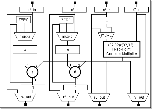
Figure 2: Butterfly/MAC Module Block Diagram
Processor Status Register (PSR)
| b1,b0 | select the functionality of the "s" adder: 0:s1+s2, 1:s1-s2, 2:s2-s1 | |
| b3,b2 | select the functionality of the "d" adder: 0:d1+d2, 1:d1-d2, 2:d2-d1 | |
| b5,b4 | select the "a" multiplexor output: 0:<zero>, 1:r4, 2:s3 | |
| b7,b6 | select the "b" multiplexor output: 0:<zero>, 1:r4, 2:s3 | |
| b8 | select the output shift amount for the "s" and "d" adders: 0:no shift, 1:shift right by 1 | |
| b9 | enables rounding logic in the "s" and "d" adders | |
| b10 | enable automatic loading of r4 with the values that are loaded into r5 | |
| b12,b11 | select the action that will be triggered by the loading of r7 with a value: 0:no action, 1: load r6 with the same value as r7, 2: if r7 was loaded via an index addressing mode then load r6 from DataROM via @x0+ indexed addressing, else r6 will become undefined; also, loading register r7 with a value always triggers automatic loading (updating) of the internal MAC "a", "b", "q" ,"r" and "L" registers | |
| b14,b13 | select the complex multiplier operation: 0:r6*r7, 1:Conjugate(r6)*r7, 2:r6*Conjugate(r7), 3:Re(r6)*Re(r7), Im(r6)*Im(r7) |
|
| b16,b15 | select the multiplier output scaler: the scaling factors are subject to customization | |
| b17 | select the r4_out and r5_out multiplexors' output: 0:r4_in/r5_in, 1:q/r | |
| b18 | select the r6_out and r7_out multiplexors' output: 0:r6_in/r7_in 1:multiplier's output | |
| b19 | select the MAC mux-L multiplexor output; 0:r6_in, 1:L register | |
| b20 | by writing a "1" into this bit the a, b, q, r, and L internal registers are cleared, and also the MAC-saturation-accumulation and s3-or-d3-big-numbers-accumulation status bits are cleared; this bit is always read as 0 | |
| b21 | enable ALU saturation functionality associated with the add, sub, sbx, sll instructions | |
| b23 | DataRAM write-back buffer empty flag bit. | |
| b24,b25 | real and imaginary s3-or-d3-big-number-accumulation flags. These bits are re-actualized whenever r7 is loaded with a value: they are set when the s3 or d3 outputs (the real and imaginary parts respectively) are outside the [-0.5,0.5) fixed-point interval, and they are reset via psr bit b20. Thus these bits behave as accumulator bits. | |
| b29,b28 | real and imaginary part MAC-saturation-accumulation flags; these flags are read-only bits, and they accumulate the MAC-saturation-occurred condition each time r7 is loaded with a value | |
| b31,b30 | ALU real and imaginary part saturation flags; these flag bits are read-only, and are set/reset by the ALU after some arithmetic operations |
Butterfly/MAC Remarks
- This module has been designed to accelerate the FFT, iFFT, FIR, and LMS-update algorithms.
- The multiplier's output can be configured to arithmetic-shift the result left or right by a set of customizable positions. This option has been included to help accommodating data types that have a precision smaller than 32 bits, and also to ease the implementation of the LMS-update algorithm. The CDSP-k2 provides the no shift / arithmetic left-shift by the value specified in the dsr register (positive or negative) options. If an overflow occurs as a result of the output's left-shift, the result saturates and the MAC saturation condition is signaled in the psr register.
- The multiplier can work as either a complex multiplier (with various input arguments conjugation options as defined by the corresponding psr bits), or as a dual parallel multiplier (performing separate RexRe and ImxIm multiplication: in this case the inputs will be interpreted as pairs of real, fixed-point numbers rather than complex numbers). Given the general architecture of the processor and instruction set, this allows the CDSP-k2 to process in parallel two rows of real fixed-point data (for most of the other arithmetic operations, it is only the programmer's interpretation of the results that differentiate a real-numbers pair from a single complex number).
- Given the multiplier input values interval of [-1,1), a "+1" value may result from the multiplication. This value is immediately converted inside the multiplier to the largest possible fixed-point number, and a MAC-saturation condition is signaled.
- Given the fact that the multiplier can operate on complex numbers, its output will have a (-2,2) range of values. This lead to implementing the data paths form the multiplier's output to the "s2" and "d2" inputs as a 33-bit bus (the "s1" and "d1" inputs are sign-extended inside "s" and "d" to 33 bits). The "s" and "d" modules always saturate their output result.
- The multiplier precision is a customizable parameter. Even though the processor word is 32 bits wide, the multiplier can truncate the inputs to a lower precision and deliver a smaller than 63-bit signed result. The customizable multiplier output shift options can retain the 32 high-order bits of the result, or it can retain lower order result bits while saturating if the result is out of the reduced range. The CDSP-k2 uses a 17x17=33 bits signed multiplier.
- In order to allow lower precision data types, the "s" and "d" adders can be featured with a customizable number of rounding options (for example, for 16-bit fixed-point numbers accommodation, a 2^-17 rounding constant may be programmed to be added under a psr bit control). The CDSP-k2 provides the 2^-17 rounding option.
FFT Inner Loop Assembler Example
The key element in performing the FFT algorithm is repetitive butterfly calculation. The following example assumes a maximum 3-stage pipelined multiplier and single-cycle "s" and "d" modules. The x2 and x3 index registers are assumed to be programmed in bit-reverse operation mode, and x0 ConstantsROM pointer is assumed to fetch the twiddle factors in the necessary order; the psr is assumed to be programmed for FFT operation (i.e. b10 set and b12-b11 set to mode 2, see psr bits); also, the x2 pointer is assumed to point one-step behind x3 (inside each loop it is used to store the previous butterfly calculation results).
lda r5,@x3*;  r4-in <= Ram[x3], r5-in <= Ram[x3],         // load the first of the butterfly input data
              x3 <= BitReverseInc(x3);                    // and move the x3 pointer to next input data
lda r7,@x3*;  a <= r4-in, b <= r5-in                      // load a and b registers from r4 and r5 inputs
              q <= s3, r <= d3,                           // save the previous step's calculation results
              r6-in <= DataRom[x0], r7-in <= Ram[x3],     // load the second of the butterfly input data
                                                          // and the butterfly coefficient
              x0++, x3 <= BitReverseInc(x3);              // move x0 to next coef and x3 to next input
sta r4, @x2*; Ram[x2] <= r4-out, x2 <= BitReverseInc(x2); // store the saved previous calculation's
sta r5, @x2*; Ram[x2] <= r5-out, x2 <= BitReverseInc(x2); // results (x2 pointer is one step behind x3)
Memory Model:
The memory model plays an essential role in the CDSP functionality. Since the processor makes no distinction between integer and fixed-point complex number words, it is only the memory organization that permits transparent usage of all instructions with both data types: the linear addressing space of both RAM and DataROM is divided in two separate regions, one for fixed-point complex numbers, and one for integer numbers. (each of these two regions can be further divided into a simple precision area and an extended precision area if needed). The functionality of these regions is defined as follows.
The Extended Precision Memory
Since the processor uses internally the extended precision representation for numbers, the operations on extended precision memory areas will not generate precision-related problems. The extended-precision, integer to complex and complex to integer conversions obey the following guidelines:
For both RAM and DataROM, when an 32-bit integer number word is read by a complex operand(s) instruction, the binary pattern of the integer word is copied in the real part of the complex operand (and will be interpreted according to the fixed-point representation of signed numbers), while the imaginary part of the complex operand is generated ad-hoc as zero.
Assembler example:
.var @IntegerArea IntVar   ; declare IntVar inside the integer numbers RAM area
     lda r0,IntVar         ; the IntVar is loaded in the real part of r0 and will be interpreted as a
                           ; fixed-point number; the imaginary part is loaded with zero.
For RAM writes, when a fixed-point complex number word is stored in the integer RAM area, its imaginary part is discarded and its real part is stored in RAM; the bit pattern of its real part will be interpreted as a 32-bit integer real number.
Assembler example:
.var @IntegerArea IntVar   ; declare IntVar inside the integer numbers RAM area
     sta r0 IntVar         ; the imaginary part of r0 is discarded and the fixed-point real part of r0
                           ; that is stored in memory will be interpreted as an integer number.
For both RAM read/write and DataROM read accesses, when an integer memory word is accessed by an integer operand(s) instruction, the word is used by the instruction as-is; also, when a fixed-point complex memory word is accessed by a fixed-point complex operand(s) instruction, the word is used by the instruction as-is.
The Simple Precision Memory
If simple-precision memory areas are needed, there will be a precision loss when converting an extended precision number to simple precision (because the conversion will simply eliminate the least significant bits from the original extended precision number).
Remark
Because this conversion keeps the most significant bits of the numbers,
it only works on the fixed-point representation; it cannot be applied
to binary numbers that represent integers (there is no trivial way to
store a number held in a register and that is representing an integer
into a simle precision memory area, because this operation would loose
the least significant bits of the integer number).