|
|
|
 |
Register Model:
The CDSP-k3 is a stripped-down (and slightly modified) derivative of
the CDSP family's basic architecture. Following is an architectural
description applicable to the CDSP-k3 customization option.
The r0 and r1 registers are 32 bits wide, but they can accommodate 32+4
bit extended-integer numbers via a register mapping technique: this is
accomplished by mapping the 4-bit extensions of r0 and r1 into
registers r4 and r5 respectively; r4 and r5 are read/write registers
and they provide the way of manipulating the 4 extended-word bits.
Registers r0, r1, r4, and r5 behave like ordinary 32-bit, and
respectively 4-bit, registers in conjunction with most operations,
except for a specific subset: when r0 or r1 is one of the operands in
an addition or subtraction, it will be padded with r4 or respectively
r5 before the operation is performed, and the result of the operation
will be split into a 32-bit low part going in the 32-bit r0 or r1, and
a 4-bit high part going to the 4-bit r4 or respectively r5.
The r2 and r3 integer registers are 16 bits wide.
The m register is the multiplier's first operand, and also the
multiplier result register. It is 32 bits wide.
Index register x0 is the DataROM pointer; it is 14 bits wide (for 16KW
DataROM).
Index registers x1, x2, and x3 are the RAM pointers; they are 10 bits
wide (for 1KW offset addresses).
Index base registers b1, b2, and b3, and limit registers L1, L2, and L3
are used by the various indexed addressing modes; they have the same
width as the RAM index registers (see following sections).
The bar (base address register) is used in the biased addressing modes
(see following sections). It is 12 bits wide (for a 4KW RAM).
The pcr (program counter register) is the instruction pointer. It is 12
bits wide (for 4KW CodeROM).
The rsr (return from subroutine register) holds the return address of
the last subroutine call; it is the programmer's responsibility to save
it (stack it) if nested calls are needed. It has the width of the pcr.
Ports p and q are the processor communication ports; each port is
implemented as a pair of unidirectional data paths, one for data input
and one for data output (i.e. the processor actually hosts a p-in, a
p-out, a q-in, and a q-out port, each of which being configurable to
have different widths). Thus, in order to attach an external ROM table
to port p, p-out can be connected to the ROM address bus, and p-in can
be connected to the ROM data bus: p-out is 14 bits wide and p-in is 16
bits wide for a 16Kx16 external ROM).
Port k is the control and synchronization port (it's also implemented
as a pair of unidirectional data paths).
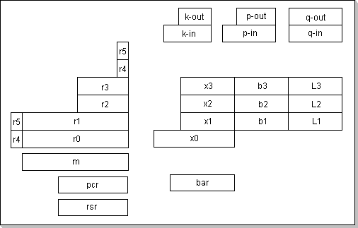
Figure 1: CDSP-k3 Registers (Programming Model)
Addressing Modes:
The instruction set is based on the two-operand model, one of them residing in a processor register, and the other residing in memory: RAM or DataROM (the CodeROM cannot be accessed as data). Most of the two-operand instructions follow this model, while most of the one-operand instructions operate on the internal registers only. These rules generate a highly orthogonal instruction set; however, some special-purpose instructions make exception from these rules (see following sections).
Following is a detailed description of the various addressing modes, accompanied by a number of relevant assembler examples.
Implied addressing:
This mode is used by instructions that either have no operand, or the
operand is implicitly specified by the instruction itself. Although the
basic processor instruction set only uses this mode for the "nop" and
"brk" control instruction, it is a useful option when implementing
application-specific instructions.
Assembler syntax example:
nop;            no operation (dummy instruction)
Direct addressing:
This mode specifies the data to be accessed by an instruction via its
address embedded in the instruction code. Both RAM and DataROM can be
accessed via this addressing mode. Depending on the operand type, the
assembler generates the correct instruction code format (RAM/DataROM
reference).
Assembler syntax example:
.cst k0: 123    ;declare a constant, allocate a DataROM address for it, and define it as being 123
.var v0         ;declare a variable and allocate a RAM address for it.
lda r0,k0       ;r0 will be loaded with 123 (the k0 constant's address is supplied in the op-code)
lda r1,v0       ;r1 will be loaded with v0 (the contents of the RAM location where v0 is allocated)
Remark:
The processor doesn't support in hardware the usual "immediate"
addressing mode; the assembler is responsible for converting the usual
assembler syntax specifying the immediate addressing mode into the
processor's DataROM direct addressing mode (a DataROM access is
inferred from the "immediate" mode):
lda r0,123      ;r0 will be loaded with the integer 123:  r0 = 123
                ;The assembler actually allocates an address in the DataROM, places the 123
                ;constant in that location, and includes its address in the op-code.
Indexed addressing:
This mode specifies the data to be accessed by an instruction via its
address held in an index register. Both RAM and DataROM can be accessed
via this addressing mode. Depending on which index register is used to
point to the data, either the RAM or the DataROM is targeted.
Assembler syntax example:
lda r0,@x0      ;the DataROM location pointed by x0 is loaded into r0:  r0 = DataROM[x0]
lda r1,@x1      ;the RAM location pointed by x1 is loaded into r1:  r1 = RAM[x1]
Remark :
The index addressing mode is complemented with a number of related
features designed to enhance data access on typical DSP applications
(see following sections).
Indexed addressing variations:
Each of the index registers accommodates a number of features used when
addressing an operand; however, these features are not common to all
the index registers, but rather differentiate their functionality.
Index register x0 DataROM pointer is only featured with the
post-increment-by-one option; no wrap-around functionality is provided.
Index registers x1 and x2 RAM pointers are featured with
post-increment-by-one and post-decrement-by-one options; wrap-around
functionality is provided by means of two related registers: base
b1(b2) and limit L1(L2). The wrapping algorithm is as follows: first
the data is accessed (via the post-increment / post-decrement
addressing); then the index register is compared against its
corresponding L register: if the values match the index register is
initialized with its corresponding b register, else it is updated
according to the mode (+/- 1).
Index register x3 RAM pointer is featured with variable-amount
post-increment. Register r3 (its corresponding low bits) is used as a
signed variable increment. The wrapping algorithm uses the x3's
corresponding b3 and L3 registers, and is the same as for x1 and x2.
Assembler syntax example:
lda r0,@x0+     ;r0 = DataROM[x0],  x0++;
lda r1,@x1+     ;r1 = RAM[x1], x1 = (x1 == L1 ? b1 : ++x1);
lda r2,@x2-     ;r2 = RAM[x2], x2 = (x2 == L2 ? b2 : --x2);
lda r0,@x3+     ;r0 = RAM[x3], x3 = (x3 == L3 ? b3 : x3+RelevantBits(r3));
Remark 1:
The relation between the index registers' limit (L) and base (b)
corresponding registers depends on the sign of the increment: it is up
to the programmer to ensure that for a positive increment L>b, while
for a negative increment L<b. This is true both when differentiating
between post-increment-by-one and post-decrement-by-one modes, as well
as when using the signed variable increment with x3.
Remark 2:
The x1, x2, and x3 index registers have an associated "scan address
space", as defined by their associated base (b) and limit (L)
registers. The size of the scan address space for x1 and x2 is
[ABS(Ln-bn)+1] (the "+1" term appears because the scan space includes
both address limits: b and L; i.e. the index registers take both these
limit values when cycling through the scan address space).
However, because the index registers are only checked for equality
against their corresponding limit register (L) in order to provide them
with wrap-around functionality, x3 will not wrap back to its base
address (b3) if it's passing over its limit address (L3) without
hitting it. In order to guarantee that the wrap-around will
consistently take place with x3's post-increment mode, it is necessary
to have (L3-b3) a multiple of the x3's increment (r3), and x3 must be
initialized with b3. For example, a valid configuration will be
x3InitialValue=b3=10, r3=3, L3=22; this will result in the following
address space: {10, 13, 16, 19, 22}.
Remark 3:
When loading an index register with a new value, that value is
available for use as a pointer in the very next instruction following
the index register load (i.e. there is no data-access latency). For
example:
ldx.ptr x1,100  ;x1 = 100;
lda r1,@x1      ;r1 = RAM[100];
ldx.ptr x1,200  ;x1 = 200;
lda r1,@x1      ;r1= RAM[200];
Remark 4:
There is a one-cycle latency between the moment the r3 register is
loaded and the moment when it can be used as increment with the x3
post-increment addressing mode; there is no guaranteed functionality of
the x3 post-increment addressing mode in the latency cycle (note
however that this abnormal behavior of the r3 register is only related
to its use as an increment with the x3 post-increment mode). For
example:
lda r3,3        ;r3 = 3; (but r3 cannot be used as increment yet)
ldx.ptr x3,300  ;x3 = 300; (from now on now r3's value when used as increment is guaranteed to be 3)
lda r0,@x3+     ;r0 = RAM[300], x3 = (x3 == L3 ? b3 : x3+3);
Biased addressing:
The bar register is a special purpose pointer that can be used to bias
both direct and indexed addressing modes, but only in conjunction with
RAM accessing (DataROM accesses cannot be biased). All the
previously-discussed RAM addressing modes (and variations) have both
the biased and non-biased options.
Biased direct addressing mode:
When the bar register is used in conjunction with direct addressing,
the address supplied in the op-code is used as an offset (relative to
the bar) for accessing the data. This allows for a small address-field
in the operation code, while still enabling access to a large address
space by using a wide bar register. The address offset is interpreted a
signed number that is added to the bar register in order to provide the
final data address.
Assembler syntax example:
.var @10 v10    ;declare a variable by specifying it's address to be 10 (RAM location).
lda r1,bar:v10  ;r1 = RAM[bar+10]  // (v0 is interpreted as an offset; it can be seen as a local variable).
Biased indexed addressing mode:
When the bar register is used in conjunction with the index addressing
modes, the address held in the index registers is used as an offset
(relative to the bar) when accessing the data. The index register is
interpreted as a signed number that is added to the bar register in
order to provide the final data address.
Assembler syntax example:
ldx.ptr x1,10   ;load index register x1 with 10.
ldx.ptr x2,20   ;load index register x2 with 20.
lda r1,@bar:x1  ;load memory location RAM[bar+10] into r1.
lda r2,@bar:x2+ ;load memory location RAM[bar+20] into r2, then update x2.
Indirect addressing:
The indirect addressing mode is only used by a small group of
instructions. It is a convenient way of reducing the number of bits
necessary to provide a branch target address (by specifying a RAM
location that contains the branch address, instead of specifying the
CodeROM address itself). This scheme also allows for calculated-address
branches, and makes possible the creation of return-address stacks in
RAM.
Assembler syntax example:
.var VariableBranchAddr   ;a number representing a CodeROM addr has to be placed in this var.
bri @VariableBranchAddr   ;the branch's CodeROM target address is now taken from this variable.
Instruction Set:
Table 1 lists the CDSP-k3 instruction set, together with the addressing modes applicable to each instruction.
Notations used in the instruction set table:
r - accumulator registers (r0 - r5)
x - index registers (x0 - x3)
p - communication ports (p and q ports)
t - memory operand, using any of the available addressing modes
(immediate, direct, indexed variations)
n - shift amount: 1,2,3,4 (or any other group of four fixed values)
j - jump (and subroutine call) CodeROM address
N - immediate addressing mode (this is a pseudo addressing mode; the
assembler converts it to direct mode)
R - register operand
D - direct addressing mode
X -index addressing modes (and variations)
J - jump (and subroutine calls) CodeROM addressing
| Instruction Name | Mnemonic | Description | Addr. Modes | Remarks |
| No Operation | nop | pcr++ | - | - |
| Logic AND | and r,t | r &= t; pcr++ | N D X | - |
| Logic Inclusive OR | Ior r,t | r |= t; pcr++ | N D X | - |
| Logic Exclusive OR | xor r,t | r ^= t; pcr++ | N D X | - |
| Addition | add r,t | r += t; pcr++ | N D X | - |
| Subtraction | sub r,t | r -= t; pcr++ | N D X | - |
| Reverse Subtraction | sbx r,t | r = t-r; pcr++ | N D X | 1 |
| Shift Left Logic Register | sll.n r | r <<= n; pcr++ // n=1,2,3,4 | R | - |
| Shift Left Logic Location | sll.n r,t | r = t << n; pcr++ | N D X | 2 |
| Shift Right Logic Register | srl.n r | r >>= n; pcr++ | R | - |
| Shift Right Logic Location | srl.n r,t | r = t >> n; pcr++ | N D X | 2 |
| Shift Right Arithm Register | sra.n r | r >>>= n; pcr++ | R | - |
| Shift Right Arithm Location | sra.n r,t | r = t >>> n; pcr++ | N D X | 2 |
| Load Accumulator | lda r,t | r = t; pcr++ | N D X | - |
| Store Accumulator | sta r t | t = r; pcr++ | D X | - |
| Load Multiplier Register | ldm t | m = t; pcr++ | N D X | 3 |
| Multiply | mul t | m *= t; pcr++ | N D X | 3 |
| Store Multiplier Result | stm t | t = m; pcr++ | D X | 3 |
| Multiply Sign | sgn r,t | r *= sgn(t); pcr++ | N D X | 4 |
| Test if Equal | teq r,t | Cmpf &= (r == t); pcr++ // Internal flag |
N D X | 5 |
| Test if Not Equal | tne r,t | Cmpf &= (r != t); pcr++ | N D X | 5 |
| Test if Greater | tgr r,t | Cmpf &= (r > t); pcr++ | N D X | 5 |
| Test if Greater or Equal | tge r,t | Cmpf &= (r>= t); pcr++ | N D X | 5 |
| Test if Smaller | tsm r,t | Cmpf &= (r < t); pcr++ | N D X | 5 |
| Test if Smaller or Equal | tse r,t | Cmpf &= (r <= t); pcr++ | N D X | 5 |
| Test by Bitwise AND | tbw r,t | Cmpf &= (r & t); pcr++ | N D X | 5, 6 |
| Branch Always | bra j | pcr = j | J | - |
| Branch if True | brt j | Cmpf ? pcr = j : pcr++ | J | 7 |
| Branch if False | brf j | Cmpf ? pcr++ : pcr = j | J | 7 |
| Branch Indirect | bri @t | pcr = RAM[t] | D X | 8 |
| Cycle | cyc r,@t | - -r ? pcr = RAM[t] : pcr++ | D X | 9 |
| Hardware Repeat | rpt r,@t | D X | - | |
| Jump to Subroutine | jsr j | rsr = ++pcr; pcr = j | J | 11 |
| Store rsr register | sts.rsr t | t = rsr; pcr++ | D X | - |
| Load bar register | lds.bar t | bar = t; pcr++ | N D X | - |
| Store bar register | sts.bar t | t = bar; pcr++ | D X | - |
| Add to bar register | add.bar t | bar += t; pcr++ | N D X | 12 |
| Load comm port from mem | lds.com p,t | p-out = t; pcr++ | N D X | 13 |
| Store comm port to mem | sts.com p,t | t = p-in; pcr++ | D X | 13 |
| Load control port from mem | ctl t | k-out = t; pcr++ | N D X | 13 |
| Hardware Directed Break | brk | - | 14 | |
| Wait for Condition | wai t | N D X | 15 | |
| Register xfer to index pointer | xfr.ptr x,r | x.ptr = r; pcr++ | R | 16 |
| Load index pointer | ldx.ptr x,t | x.ptr = t; pcr++ | N D X | 17 |
| Store index pointer | stx.ptr x t | t = x.ptr; pcr++ | D X | 17 |
| Load index base | ldx.bas x,t | x.bas = t; pcr++ | N D X | 17 |
| Load index limit | ldx.lim x,t | x.lim = t; pcr++ | N D X | 17 |
Table 1: CDSP-k3 instruction set
Table 1 Remarks:
- The "sbx" instruction can be used for negating a number:
sbx r0,0
- The memory location shift instructions can be used to cut one
cycle when having to shift a memory location by embedding the shift
into the memory load:
     srl.4 r0,VariableToShift
sta r0 VariableToShift - "m" is the multiplier in/out register: first m is loaded with one
of the multiplication operands, then the "mul" instruction is issued,
and after N cycles the result is ready back in the m register:
     ldm MultOp1
     mul MultOp2
     [...]
stm MultReslt - The "sgn" instruction can be used to obtain the absolute value of
a register or variable:
.var Tmp
     sta r0 Tmp
sgn r0,Tmp - The various test instructions use an internal processor flag Cmpf
that can be used for chaining. All non-test instructions set this flag
to "1". This mechanism provides an easy way for checking if a variable
belongs to an interval, is outside an interval, etc. (Note that in
order to use this mechanism it is necessary to place the successive
test instructions right one after the other)
     [NonTestInstruction]
     tge r0,10
     tse r0,20
     brt ValueIsIn10to20
ValueIsOutside10to20:
     [r0 < 10 or r0 > 20]
     bra Continue
ValueIsIn10to20:
     [10 <= r0 <= 20]
Continue: - The "tbw" bitwise-AND test provides a way for testing individual
bits:
     tbw r0,1
     brt Bit_b0_of_r0_set
Bit_b0_of_r0_reset:
     [...]
     bra Continue
Bit_b0_of_r0_set:
     [...]
Continue: - The brt and brf instructions check the chain-ANDed Cmpf flag. These instructions take 2 cycles when taken and 1 cycle when not taken. Note that the conditional branch instructions have to be chained with the test instructions (i.e. they placed right after the test instruction(s)).
- The "bri" instruction provides a way to jump to a pre-calculated
address. It can be used for returning from a subroutine:
SubrStart:
.var TMP_ReturnAddress
     sts.rsr TMP_ReturnAddress
     [SubroutineBody]
bri @TMP_ReturnAddress - The cycling "cyc" instruction condenses a counter register
decrement, the counter testing, and a conditional branch into one
instruction. It takes two cycles when the branch is taken, and one
cycle when the branch is not taken. Only the indirect addressing mode
is provided for specifying the destination address: the instruction
argument is a pointer to a memory location that contains the actual
branch address (i.e. the branch is indirect, same as with the "bri"
instruction).
By modifying the counter register inside the loop, the number of times the loop is executed can be changed as a result of calculations performed within the loop.var TMP_LoopingAddress
lda r2,&Loop
sta r2 TMP_LoopingAddress
lda r2,LoopCount
Loop:
[LoopBody]
cyc r2,@TMP_LoopingAddress - The hardware repeat "rpt" instruction provides a way to execute a
loop for a pre-calculated number of times, without having the
possibility to change the loop-counter within the loop body. Hardware
loops cannot be nested: they are intended for use in the innermost
level of nested loops. Hardware loops have a zero-cycle penalty as
compared with their corresponding linear code (i.e. the counter
decrement, its testing, and the branch at the ending of the loop do not
require any additional clock cycles).
The initialization of the loop is as follows: first a counter register has to be loaded with the RepeatCount-1 value, where RepeatCount is the number of times the looping is needed; then the repeat instruction has to be inserted in the code; then a one-instruction slot has to be inserted in the code; the loop body begins right after this instruction; the ending of the loop is specified indirectly in the "rpt" instruction code. Unlike with the "cyc" instruction, modifying the loop counter register inside the loop will not affect the number of times the loop is executed; this is because all the loop-related internal registers (counter, start-address, ending-address) are initialized at the moment the "rpt" instruction is executed..var TMP_LoopEndingAddress
lda r2, &LoopEndingAddress
sta r2 TMP_LoopEndingAddress
lda r2 RepeatCount
add r2 –1
rpt r2 @TMP_LoopEndingAddress
nop
LoopStartAddress:
[FirstInstructionInTheLoop]
[...]
LoopEndingAddress:
[LastInstructionInTheLoop] - The "jsr" instruction provides a way to save a "return address"
in order to be used in (nested) subroutine calls. However, since this
instruction saves the "return address" in a register (the "rsr"), thus
overwriting any previously saved address, it is up to the programmer to
save it in memory if needed. Indexed modes can be used to generate a
simple stack structure, or the "bar" register can be used to generate
complex subroutine activation structures.
.var Stack[StackSize]
     ldx.ptr x1, &Stack
     jsr SubrEntry
     [RestOfTheProgram]
SubrEntry:
     sts.rsr @x1+
     [SubroutineBody]
     sts.rsr @x1-
bri @x1 - The "add.bar" instruction is provided to ease the use of the "bar" register as a base-pointer. The argument of this instruction is interpreted as a signed number, thus allowing to build stack structures.
- The "lds.com" and "sts.com" instructions are the equivalents of the generic microprocessor "in" and "out" instructions: "lds.com" correspond to "out"s, and "sts.com" correspond to "in"s. The "ctl" instruction is also an "out", but its destination is the processor control output port (k-out).
- The "brk" instruction provides a way to direct the program flow according to the processor control input port (a relevant group of bits of k-in) . This is meant to complement the data-transfer based way of interaction between the processor and the peripherials (the communication ports instructions).
- The "wai" wait instructions stalls program execution and waits
for a specified bit-pattern at the processor control input port (a
relevant group of bits of k-in). This provides a way of synchronizing
the processor with external events, thus complementing the
communication ports instructions and the break instruction. This
instruction can also be used to test some internal processor flags and
wait until an internal condition is met. The multi-cycle multiplier
provides a "multiplier ready" bit that can be used to synchronize
program execution with the multiplier.
     ldm MultOp1
     mul MultOp2
     wai MultiplierReady
stm MultResult - The register transfers are only allowed between a specific set of registers: the index registers pointers (but not their corresponding limit and base registers) can be loaded from exactly one accumulator register. The rule is that xN.ptr can be loaded only from rN (x0.ptr from r0, x1.ptr from r1, x2.ptr from r2, and x3.ptr from r3). No other register-transfers are included in the instruction set.
- The index registers components (xN.ptr pointers, xN.bas bases, and xN.lim limits) can be loaded from memory using any of the addressing modes, but only the index pointers (xN.ptr) can be stroed in memory. Since the base and limit components of the index registers cannot be modified by any other instruction, the values used to load them can also be stored in a separate location (at the very moment they are loaded) for further reference.
Memory Model:
The memory model plays an essential role in the CDSP functionality; it should be defined (customized) according to the specific algorithm that has to be implemented. Since the processor does not feature any special instructions to cope with the different sizes of memory words (it makes no distinction between 16-bit and 32-bit words), it is only the memory organization that permits transparent usage of all instructions with both data types: the linear addressing space of both RAM and DataROM is divided in three separate regions, two 16-bit word region, and one 32-bit word region. The functionality of these regions (three RAM and three DataROM) is defined as follows:
For both RAM and DataROM, when a 16-bit word is read by a 32-bit operand(s) instruction, the word is either left-padded with zeroes or sign-extended, depending on which of the two 16-bit regions it resides in.
Assembler example:
.var @SignExtendRAM16Area SxVar16  ; declare SxVar inside the 16-bit sign-extending RAM area
.var @ZeroExtendRAM16Area ZxVar16  ; declare ZxVar inside the 16-bit zero-extending RAM area
     lda r0,SxVar16                ; the 16-bit SxVar is sign-extended when loaded in r0
     lda r1,ZxVar16                ; the 16-bit ZxVar is zero-extended when loaded in r1
For RAM writes, when a 32-bit word is stored in any of the two (zero-extending or sign-extending) 16-bit RAM regions, its high-order bits are discarded.
Assembler example:
.var @RAM16Area Var16   ; declare a 16-bit variable (residing in any of the two 16-bit areas)
     sta r0 Var16       ; the high-order 16 bits of r0 are lost when r0 is stored in Var16
For both RAM read/write and DataROM read accesses, when a 16-bit memory word is accessed by a 16-bit operand(s) instruction, the word is used by the instruction as-is; also, when a 32-bit memory word is accessed by a 32-bit operand(s) instruction, the word is used by the instruction as-is.
Assembler example:
.var @RAM16Area Var16  ; declare a 16-bit variable (residing in any of the two 16-bit RAM areas)
.var @RAM32Area Var32  ; declare a 32-bit variable (residing in the 32-bit RAM area)
     lda r2,Var16      ; the 16-bit Var16 is loaded in the 16-bit r2
     sta r3 Var16      ; the 16-bit r3 is stored in the 16-bit Var16
     lda r0,Var32      ; the 32-bit Var32 is loaded in the 32-bit r0
     sta r1 Var32      ; the 32-bit r1 is stored in the 32-bit Var32
Remark:
The previously described method of partitioning the memory (RAM and
DataROM) is covering all the possible cases; however, if a specific
algorithm does not use a certain data type, the corresponding memory
area doesn't need to be implemented.
For example, if an algorithm uses 16-bit and 32-bit computation
(variables, intermediate results, etc.), but only uses 16-bit
constants, the DataROM doesn't need to contain a 32-bit word area;
furthermore, if the 16-bit constants are all interpreted as signed
numbers (in the algorithm's 32-bit calculations), the 16-bit
zero-extending DataROM area is not needed.