|
|
|
 |
The SDPxx is a fast cryptographic processor family designed to perform in hardware a number of frequently used data-security related algorithms. The SDP11 implements the 56-bit key DES, the 168-bit key Triple-DES, the 160-bit SHA-1, the 128-bit MD5, and the keyed HMAC algorithms.
The chip's interface is built using a 32-/16-/8-bit programmable-width bi-directional data bus, a 32-/16-/8-bit command bus, and a number of control signals. This allows easy interfacing of the chip with 16- and 32-bit processors and/or DMA controllers, and also supports the option of integrating the IP variant of the chip with an 8-bit microcontroller core (provided that the 8-bit IP core can be clocked at a sufficiently high frequency to keep up with the SDP11 execution speed).
@toc@Table of contents@
Architecture Overview
The SDP11 contains two data processors, an internal memory system used to store multiple session-context information, a DMA-based fast I/O interface, a command processor connected to the command port, and a control unit. The data processing units are accessed via the chip's bi-directional data bus. The command processor is accessed via the chip's bi-directional command bus. Following is a brief description of these building blocks, their functionality, and the way they are interconnected (see fig. 1).
The first data processing module is a DES/3DES encryption/decryption unit. It can be programmed to perform either encryption or decryption on an input data stream, using either the DES or the 3DES algorithm, in either the ECB or CBC modes of operation.
The second data processing module performs either a selectable hash function or a HMAC function on a data stream. The hash function can be implemented using either the SHA-1 or the MD5 algorithm. The data stream that is processed can be either the encryption/decryption unit's input data or its output data.
The internal memory system is used to store the two processing channels' context information at a given moment. In this way a session (characterized by its encryption/ decryption keys, its IV, its HMAC keys, etc.) can be interrupted and its state stored in a set of context memory locations for later resumption.
The command channel receives chip-programming commands issued on the command port, and dispatches them to the other on-chip channels (except for the commands targeting the command channel itself). The commands results are delivered from the result register through the bi-directional command port.
The control unit is responsible for the global chip functionality and synchronization; it generates the DMAs handshaking signals, the chip-status output signals, etc, and it monitors the chip-control inputs (apart from sharing the chip's data bus, the three DMA units are completely independent).
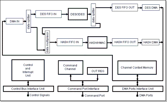
Figure 1: SDP11 Architecture
Global Control Registers
Five control registers, one command register and one output register are provided to setup the overall chip functionality on a per-frame basis. Each of these registers is 32 bits wide.
The FRMLEN register holds the length of the next frame to be processed, expressed in bytes. This register is decremented down to zero while the frame is being processed.
The FRMID register holds the frame ID number. The first action taken at the beginning of each new frame is to place this 32-bit ID word into the DES/3DES and HASH/HMAC channels' output FIFO buffers (if the corresponding control bits are set), allowing to establish the correspondence between the input data stream and the result output data streams. This is particularly useful in the case of the HASH/HMAC channel that delivers the result with a certain delay with respect to the DES/3DES channel. By using this feature, the two channels can run in parallel, and the delayed HASH/HMAC result can properly be identified.
The CMDREG register is the chip's global command register. Commands are placed on the chip's command bus and have this register as a destination.
The OUTREG is the chip's output register. Read cycles from the chip's command bus will access the contents of this register. A number of commands are provided to load this register with some of the chip's internal data and control registers.
The FRMTHR register holds a threshold value that is continuously compared with the FRMLEN countdown counter. Each transition from the condition FRMLEN<>FRMTHR to FRMLEN=FRMTHR sets the FRMINT interrupt request bit in the IRQREG register. The interrupt request generated by this register is intended to provide an early information about the current frame completion.
The IENREG register holds the interrupt enable bits for the various conditions, together with the global interrupt enable bit (the function of the bits in this register is described throughout this specification).
During the interrupt service routine, the various specific interrupt enable bits are not automatically affected (no hardware action is performed to affect them in any way), except for the global interrupt enable bit that is reset upon an interrupt acknowledge. In order to re-enable the chip's interrupt mechanism, the global interrupt enable bit has to be set by software upon completion of the interrupt service routine.
b0: global interrupt enable (it is automatically cleared when an interrupt is acknowledged)
b21: INFIFOE ien
b22: INFIFOF ien
b23: DESFIFOE ien
b24: DESFIFOF ien
b25: HASHFIFOE
b26: HASHFIFOF ien
b27: FRMINT ien
b28: DESRDY ien
b29: HASHRDY ien
b30: HASHRSLT ien
The IRQREG register holds the interrupt request bits for the various
conditions, together with the global interrupt request bit (the
function of the bits in this register is described throughout this
specification).
The interrupt mechanism is based on the following algorithm: when a
certain internal condition occurs, the corresponding interrupt request
bit is set (regardless of its prior condition) and, provided both its
corresponding interrupt enable and the global interrupt enable bits
are set, an interrupt is generated (the interrupt request signal is
asserted). The interrupt service routine has to determine in software
the originator(s) of the interrupt by checking the interrupt request
bits in this register. The interrupt request bits are not
automatically reset upon interrupt acknowledges, but rather they
should be explicitly reset in software at the entry of each specific
interrupt service routine; if an interrupt request bit is not reset,
it will generate another (false) interrupt the moment it will be
re-enabled (note that the global interrupt request bit is a read-only
bit; it is the logic "or" of all the specific irq bits).
b0: global interrupt request; this is the logic OR of all interrupt requests
b21: INFIFOE irq
b22: INFIFOF irq
b23: DESFIFOE irq
b24: DESFIFOF irq
b25: HASHFIFOE
b26: HASHFIFOF irq
b27: FRMINT irq
b28: DESRDY irq
b29: HASHRDY irq
b30: HASHRSLT irq
The DES/3DES Channel
This channel performs the DES/3DES algorithms in either ECB or CBC modes (and CBC sub-modes). Sixteen registers are responsible for the channel operation: three control registers, eight (four double-word) context registers, and five reserved. All these registers are 32 bits wide.
The DESCTL register holds the channel operation mode control bits:
b15: Channel enable
b14: FRMID enable: controls posting of the FRMID in the output buffer at the beginning of each frame.
b7: Key bits interpretation: 64-bit (parity bits included) or 56-bit key(s)
b5-b4: ECB/CBC mode (and CBC sub-mode) selector
b1-b0: DES/3DES encryption/decryption algorithm selector
The DESHDR register is used to specify how many header bytes are to bypass the channel without being processed.
b31-b0: bypass counter
The DESCNT register is used to specify the number of bytes that are to be processed by the channel in the following frame, following the ones specified in the DESHDR register that are to pass unprocessed.
b31-b0: data length
The DESIVL and DESIVH registers hold the channel Initialization Vector that is used in the CBC modes; the IV is formed by concatenating the DESIVL and DESIVH registers.
The DESKnL and DESKnH registers, where n={0,1,2}, are used to store the encryption/decryption key. DESK0L and DESK0H are concatenated to generate the simpe-DES key; similarly the DESK1L, DESK1H, and DESK2L, DESK2H are concatenated to generate the two extra keys required by the triple-DES algorithm.
The channel processes data on a frame-based model; typically, the following stages can be identified: First, the frame length and ID must be loaded into the FRMLEN and FRMID registers respectively, and the interrupt enable bits in the IENREG register must be programmed. Second, the DES/3DES channel control registers have to be programmed (according to the desired operation to be performed during the next-to-come frame). Third, a GOFRAME command has to be issued to the CMDREG command register. This final step will initiate the frame processing sequence: First the FRMID is placed in the output FIFO buffer if the FRMID-enable control bit is set; then the input DMA starts requesting data that is fed to the DES FIFO IN, and from there into the DES/3DES processor. The output of the processor is fed into the DES FIFO OUT, and from there it's delivered on the data bus by the DES output DMA. According to the values programmed in the control registers, the first DESHDR bytes of header data will pass through the channel unprocessed; next a number of DESCNT bytes will be processed by the channel; finally, the rest of the data frame (up to a total of FRMLEN bytes) will again pass through the channel unprocessed.
The HASH/HMAC Channel
This channel performs either a simple hash function or a complete hash-MAC generation on a selectable data stream, using the SHA-1 or the MD5 algorithm. Sixteen registers are responsible for this channel operation: three control registers, eight (four double-word) context registers, and five reserved registers. All these registers are 32 bits wide, and they are similar to the ones that control the DES/3DES channel operation.
The HASHCTL register holds the channel operation mode control bits:
b15: Channel enable
b14: FRMID enable: controls posting of the FRMID in the output buffer at the beginning of each frame.
b13: Output interface mode: selects the channel's output interfacing scheme DMA vs. Rd/Wr/IRQ
b7: Key bits interpretation: 64-bit (parity bits included) or 56-bit key(s)
b5-b4: Key length selector: 56, 112, 168 or 224 bits
b3: Input data steam selector: the input DMA or DES/3DES channel output
b1-b0: SHA-1/MD5 HASH/HMAC algorithm selector
The HASHHDR register is used to specify how many header bytes are to bypass the channel without being processed.
b31-b0: bypass counter
The HASHCNT register is used to specify the number of bytes that are to be processed by the channel in the following frame, following the ones specified in the HASHHDR register that are to pass unprocessed.
b31-b0: data length
The HASHKnL and HASHKnH registers, where n={0,1,2,3}, are used to store the HMAC key. HASHK0L and HASHK0H are concatenated to generate a 56-bit HMAC key; similarly the HASHK1L, HASHK1H, HASHK2L, HASHK2H, HASHK3L, and HASHK3H are concatenated to generate the 112-, 168-, and 224-bit key lengths required by the HMAC algorithm. The simple HASH functions (SHA-1 and MD5) do not use any of these key registers.
Typically, the stages this channel is passing through in order to deliver the HASH/HMAC result are similar to the ones of the DES/3DES channel: First the frame length, ID, and the interrupt bits have to be programmed (the FRMLEN, FRMID, and IENREG global registers), then the channel-specific registers must be loaded, and finally a GOFRAME command must be issued to the CMDREG command register in order to initiate the processing of a data frame. The data that is to be processed by this channel takes the following path: First the FRMID is placed in the output FIFO buffer if the FRMID-enable control bit is set; then the input data is fed into the HASH FIFO IN from either the input DMA interface or from the DES/3DES channel's output (as specified by the data-source control bit), and from there it is placed at the HASH/HMAC processor input. From the processor's output the data is fed into the HASH FIFO OUT, and from there it is output on the data bus via the HASH output DMA. As for the DES/3DES channel, only HASHCNT bytes will be processed: the first HASHHDR header bytes and the frame's trailing bytes (i.e. the last FRMLEN-HASHCNT-HASHHDR bytes in the frame) are not processed.
This channel's output interface can be programmed to work in either DMA mode or as a standard port (because this channel generates a relatively small result -up to ten 32-bit words per data frame- for some applications it may be too expensive to have a separate DMA channel allocated for it). When the interface is used as a standard port, its pins are reassigned and an interrupt-based communication protocol is defined: whenever a new result becomes available in the channel's output buffer, the port generates an interrupt (via one of its interface signals) that should launch a data-retrieval subroutine (using standard-port reads). This interrupt request pin is also reflected in the HASHRSLT irq bit in the IRQREG global register.
Parallel Frame Processing
The chip architecture allows data to be processed in parallel by the
DES/3DES and HASH/HMAC channels. Depending on the way the two
channels' control registers are programmed, an encryption or
decryption operation can be performed in parallel with the plain-text
or cipher-text hashing or HMAC calculation.
Typically, the programming sequence for parallel channel operation
will be similar to the one used to activate any of the two individual
channels; however, both channels' control registers will be programmed
together, and both channels will be enabled before the effective frame
processing will be started: First, the global per-frame chip behavior
will have to be setup by programming the global FRMLEN, FRMID, FRMTHR,
and IENREG registers. Then, each channel's control and context
registers will be programmed. Finally, the GOFRAME command will be
issued to the CMDREG, thus triggering the frame-processing sequence
that will be carried out in parallel by the two channels.
The Channel Context Memory
As described in the previous sections, 16 channel-specific 32-bit registers control the operation of each of the two channels, leading to a total of 32 channel-specific 32-bit registers. The context memory is organized accordingly as an array of 32-register sets, each of the registers in a set being 32-bit wide. The number of context memory register sets is customizable upon request, the default configuration being a 32-set array. Thus, 32 different channel-configurations can be simultaneously stored in the context memory.
Each of the context memory sets can be loaded either from outside the chip with session-startup configuration values, or directly from the internal channel-specific registers with the intermediate values that occur during a session. In this way a session can be broken in parts, since the state of the processor can be saved in a context memory register set at each interruption, and reloaded when the session is resumed.
The FIFO Buffers
Each of the three FIFO buffers has a set of two control registers used to program the way these buffers generate their output status signals and their interrupt requests.
The INFIFOFTHR, DESFIFOFTHR, and HASHFIFOFTHR threshold registers
control the generation of the corresponding FIFOF (FIFO full) signals,
together with the associated FIFOF irq bits in the IRQREG.
When the number of bytes in a FIFO is larger then the value specified
in its corresponding FIFOFTHR threshold register, the FIFOF status bit
is set; else the FIFOF status bit is kept reset.
Also, at each transition from No-of-bytes-in-FIFO < FIFOFTHR to
No-of-bytes-in-FIFO = FIFOFTHR, the corresponding FIFOF irq bit in
IRQREG is set. This allows accumulating the FIFOF interrupt requests,
but it requires the irq bit to be explicitly cleared by software.
The INFIFOETHR, DESFIFOETHR, and HASHFIFOETHR threshold registers control the generation of the corresponding FIFOE (FIFO empty) signals,together with the associated FIFOE irq bits in the IRQREG.
When the number of bytes in a FIFO is smaller then the value specified in its corresponding FIFOETHR threshold register, the FIFOE status bit is set; else the FIFOE status bit is kept reset.
Also, at each transition from No-of-bytes-in-FIFO > FIFOETHR to No-of-bytes-in-FIFO = FIFOETHR, the corresponding FIFOE irq bit in IRQREG is set. This allows accumulating the FIFOE interrupt requests, but it requires the irq bit to be explicitly cleared by software.
The HASH FIFO buffer has a separate HASHRSLT irq bit associated with it in the IRQREG, that is only meaningful when the non-DMA mode is selected for the port. This bit is set each time the HASH FIFO is loaded with a new HASH/HMAC result, i.e. it is set together with the port's specific irq signal, but unlike the port's irq, it is not reset by the port-specific interrupt acknowledge pin; it has to be reset by software.
The Command Channel
All the chip's programming is performed by issuing commands to the CMDREG command register. Following is a brief description of the command classes:
Loading the chip's internal registers is accomplished by issuing a LOADREG <RegisterSelector32> <Value32_0> ... <Value32_n> command. The RegisterSelector32 word contains 32 flag bits, each specifying whether or not a corresponding chip register is to be loaded from the command arguments list.
Loading directly register images in one of the context memory sets is performed in a similar way, via the LOADMEM command, by specifying both the destination register images and the destination register set: LOADMEM <set#> <RegisterSelector32> <Value32_0> ... <Value32_n>.
Apart for loading registers with specific values, bit operations can
be performed by using a dedicated set of three commands; however,
unlike the register loads, these commands operate on one register at a
time only. These bit-wise commands are particularly useful when
manipulating the interrupt registers.
ANDREG <reg#> Value32: this performs a logic "and" on the
register with Value32
IORREG <reg#> Value32: this performs a logic "or" on the
register with Value32
XORREG <reg#> Value32: this performs a logic "xor" on the
register with Value32
Reading the registers' values is performed by sending a READREG <RegisterSelector32> command. The RegisterSelector32 word has the same format as the one used in the LOADREG command (it contains 32 flag bits, each specifying whether or not a corresponding chip register is to be output on the command port's bus). The registers specified in the RegisterSlector32 are successively output to the OUTREG each time the OUTREG is being read; in this way a stream-reading of the chip's internal registers is possible. If a register that is specified in the RegisterSelector32 does not allow reading, a 0 (zero) value is output.
Reading directly a register-image from one of the context memory sets is performed in a similar way via the READMEM command. Both the register set, and the registers within the register set, are specified in the memory-read command: READMEM <set#> <RegisterSelector32>.
Saving the state of the two processors (DES/3DES and HASH/HMAC) in the context memory is performed by sending a SAVESTS <set#> command; this will save all the channels' configuration information in the specified context memory set.
Reloading the channels' state from a context memory set is performed similarly, using a LOADSTS <set#> command. This will reload all the channels' configuration from the specified memory set.
Initializing a new frame processing sequence is performed by issuing
a GOFRAME command, after the chip's control and context registers have
been properly initialized.
Once a new frame processing sequence has been triggered, the chip can
accept new setup commands while it processes data. In this way the
registers' loading/updating can be done in parallel with the data
stream processing. However, the command channel will be locked if a
new GOFRAME command is received before the current frame processing is
completed. Once the command channel is locked, it will not accept any
more setup or GOFRAME commands (if issued, these commands will be
lost).
The current frame processing is abandoned when the chip receives a STOP command. This command is executed regardless of the state of the chip in the moment it is received. No internal registers are affected.
The chip can be set to enter a wait state via a WAIT <Pattern32> command. After this command is executed, the resumption of the chip's activity is triggered by a control-signals configuration that is specified by the WAIT command. This is a way to provide a hardware synchronization of the chip with external asynchronous events.
Pin Connections
Figure 2 depicts the chip's busses and control signals, counting for 99 pins apart from the Vcc and GND power supply pins.
- DB: the bi-directional data bus; this is a 32-bit wide bus.
- DBS: the data-bus sub-word selector for 16-bit or 8-bit data transfer modes; this is a 2-pin control.
- DWR: this is the data-bus' write signal. When activated a data is being written from the data bus into the chip by another master on the data bus.
- DRD: this is the data-bus' read signal. When activated a data is being read from the chip to the data bus by another master on the data bus.
- CMD: this is the command port bus. It is a 32-bit bi-directional bus.
- CWR: this is the command port write signal. When active a command is being issued to the chip.
- CRD: this is the command port read signal. When active the chip result register OUTREG is being read on the command bus.
- DMAnREQ, DMAnACK, and DMAnCLK: the DMA handshaking signals; n={1,2,3} for the input, DES/3DES output, and HASH/HMAC output respectively. For n=3, the pins' functional designation is defined according to the DMA control bit in the HASH/HMAC control register: in non-DMA mode these pins are defined as PORT3IREQ, PORT3IACK and PORT3RD.
- STS: the STS signals are custom chip-status signals that can be generated upon request. The default STS status bus configuration includes: DESLXC, DESRDY, HASHLXC, HASHRDY, INFIFOE, INFIFOF, DESFIFOE, DESFIFOF, HASHFIFOE, HASHFIFOF.
- CTL: 4-bit input signal used for chip synchronization (via the WAIT command).
- IRQ, IACK: interrupt request (output) and interrupt acknowledge (input) signals.
- DESCLK, HASHCLK, CLK: DES/3DES and HASH/HMAC channels' clocks, and the main control clock; they can be connected together (i.e. the same clock signal may be applied to both channels).
- RES: The global chip reset. Some timing restrictions apply in order to guarantee proper chip initialization.
- VCCn, GNDn: Power supply signals.
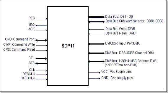
Figure 2: SDP11 Pin Connections
Feature Summary
- Hardware implementation of a multi-channel, multi-data-stream DES/ 3DES/ SHA-1/ MD5 encrypt/ decrypt/ hash/ authentication engine.
- The DES/3DES and the HASH/HMAC processors can run in parallel.
- The DES/3DES channel can be configured to run in ECB or CBC encryption/decryption modes (and some CBC variations).
- Customizable number of on-chip session context memories (default is 32), provided for fast switching of the channel-state information.
- The HMAC authentication engine can be programmed to use up to 224-bit keys.
- Configurable interrupts to signal various internal chip situations/events.
- Customizable status bus to allow continuous monitoring of the chip's internal state.
- Configurable bi-directional data bus: 8-, 16- or 32-bits wide.
- Asynchronous data transfer with respect to the chip clocks via three dedicated DMA handshaking/control ports.
- Streaming support by providing large input and output buffers.
- Configurable bi-directional command bus: 8-, 16-, or 32-bits wide; the commands results are read from the chip via the command bus.
- 3-volt operation, 5-volt tolerant.
Performance
The following numbers are referring to the reference design chip which is manufactured on a 0.35u/3.3V technology that implements fast adders and fast barrel-shifter macrocells (foundry name confidential); without these macrocells a 25% performance degradation is expected:
- DES/3DES channel: 800Mbps/250Mbps
- SHA1/MD5 channel hashing: 200Mbps
- SHA1/MD5 channel HMAC: n/a
Packaging
The chip packaging is dependent on the number of status and control
signals that result from the various possible customization options.
The SDP11 reference design chip is packaged in a 128-pin QFP package.
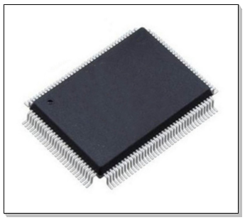
Fig.3: SDP11 reference design chip